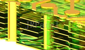
Why Are Multi-layer PCBs Mostly Even-numbered Layers?
Why are multi-layer PCBs mostly even-numbered layers and few odd-numbered layers? There are single-layer, double-layer and multi-layer PCBs. The number of layer is not limited. There are currently more than 100 layers on boards. Common multi-layer PCBs are four-layer and six-layer boards.
So everyone will have this question: Why are multilayer PCBs with even-numbered layers?
Relatively speaking, even-numbered PCBs are more than odd-numbered PCBs, and they have more advantages. Today JRPanel would like to solve this question for everyone.
Because of the fewer layer of dielectric and foil, the cost of raw materials for odd-numbered PCBs is slightly lower than that of even-numbered PCBs. However, the processing cost of odd-layer PCB is significantly higher than that of even-layer PCB. The processing cost of the inner layer is the same, but the foil/core structure obviously increases the processing cost of the outer layer.
The odd-numbered PCB requires a non-standard laminated core layer bonding process on the basis of the core structure process. Compared with the core structure, the production efficiency of factories that add foil to the core structure will decrease. Before lamination and bonding, the outer core requires additional processing, which increases the risk of scratches and etching errors on the outer layer.
There is another reason for the small number of single-layer circuit boards: single-layer circuit boards are easy to bend. When the PCB is cooled after the multilayer circuit bonding process, the different lamination tensions of the core structure and the foil-clad structure will cause the PCB to bend. As the thickness of the circuit board increases, the risk of bending of a composite PCB with two different structures increases. The key to eliminating circuit board bending is to use a balanced stack. Although the PCB with a certain degree of bending meets the specification requirements, the subsequent processing efficiency will decrease, resulting in an increase in cost. Because special equipment and craftsmanship are required during assembly, the accuracy of component placement is reduced, which will damage the quality.
To put it more easily, in the PCB process, the four-layer board is better controlled than the three-layer board, mainly in terms of symmetry. The warpage of the four-layer board can be controlled below 0.7% (IPC600 standard), but when the size of the three-layer board is large, the warpage will exceed this standard, which will affect the reliability of the smt patch and the entire product. Therefore, the general designer does not design an odd-numbered layer board, even if the odd-numbered layer realizes the function, it will Designed as a fake even-numbered layer, that is, 5 layers are designed into 6 layers, and 7 layers are designed into 8 layers.
Based on the above reasons, most multilayer PCBs are designed with even-numbered layers and few odd-numbered layers.


China PCB Manufacturer
回复删除